
This application note describes monolithic fabrication approaches for microlens arrays (MLAs), with emphasis on optical behavior, manufacturing constraints, tolerance sensitivity, and validation requirements, particularly when implemented using polymer substrates.
It is intended for optical, mechanical, and process engineers evaluating MLAs for imaging, sensing, illumination homogenization, beam shaping, and coupling applications.
This document avoids claims of universal performance and focuses on what monolithic MLAs reliably enable, where they are sensitive, and what must be validated.
What a microlens array is (engineering definition)

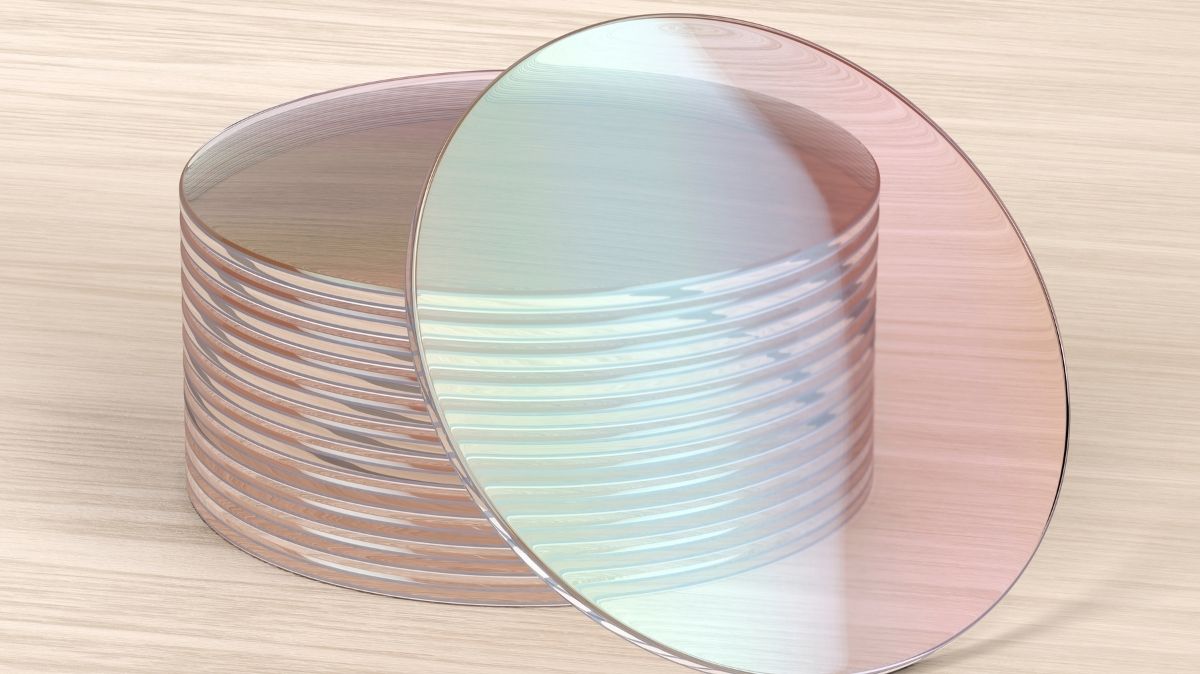
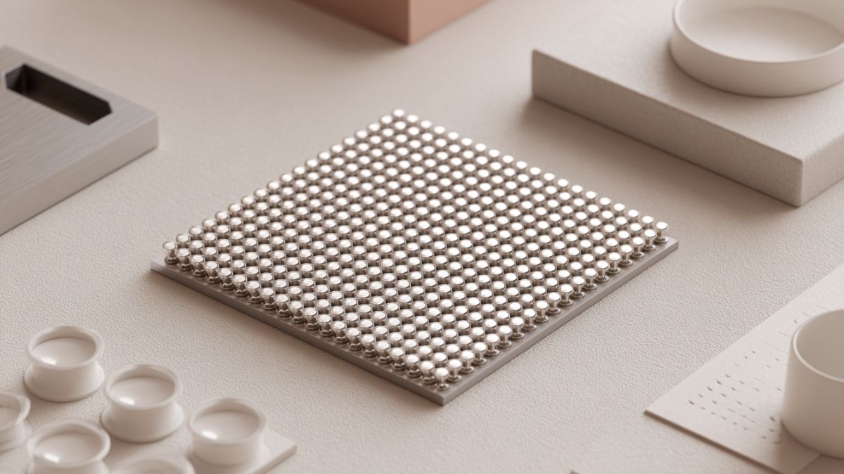
A microlens array consists of a repeating pattern of small lens elements, typically with apertures ranging from tens to hundreds of micrometers, arranged on a common substrate.
MLAs are used to:
Redistribute or homogenize light
Improve coupling efficiency
Sample wavefronts
Shape or condition beams
Performance is governed by lens geometry, pitch, fill factor, surface quality, and alignment to the optical system.
What “monolithic fabrication” means

Monolithic fabrication refers to producing:
The microlens geometry and
The supporting substrate
as a single, continuous optical component, rather than assembling discrete lens elements.
This approach eliminates inter-element assembly but does not eliminate manufacturing or alignment constraints.
Why monolithic MLAs are used
Monolithic microlens arrays are selected to:
Improve positional accuracy between lenslets
Reduce assembly steps
Improve mechanical robustness
Enable high-volume replication
These benefits are manufacturing and integration advantages, not automatic optical improvements.
Polymer substrates and monolithic MLAs
Polymer materials are commonly used for monolithic MLAs due to:
Replication efficiency
Low mass
Design flexibility
Cost advantages at scale
However, polymer substrates introduce constraints:
Higher coefficient of thermal expansion (CTE)
Lower elastic modulus
Viscoelastic behavior (creep and stress relaxation)
Sensitivity to process-induced stress
These properties influence lens shape fidelity, pitch stability, and long-term performance.
Fabrication approaches
Monolithic polymer MLAs are commonly produced using:
Precision molding
Replication from ultra-precision tooling
Lithography-assisted replication methods (application-dependent)
Achievable performance depends on:
Tool surface quality
Replication fidelity
Polymer flow and cooling behavior
Process stability
Fabrication capability is process-dependent, not guaranteed by design intent.
Optical performance considerations

Lenslet uniformity
Performance depends on:
Consistency of lenslet curvature
Pitch accuracy
Fill factor
Small deviations can produce:
Non-uniform illumination
Coupling losses
Phase or amplitude artifacts
Uniformity must be measured across the full array, not inferred from local inspection.
Surface quality and scatter
Microlens arrays are sensitive to:
Surface roughness
Tool marks
Replication artifacts
These effects can increase scatter and reduce system efficiency, particularly in imaging or sensing applications.
Tolerance and alignment sensitivity
Although monolithic fabrication fixes relative lenslet positions, MLAs remain sensitive to:
Global decenter and tilt
Axial placement relative to other optics
Rotation relative to pixel grids or emitters
Monolithic does not mean “self-aligning” at the system level.
Thermal and environmental behavior

Polymer MLAs may experience:
Focal length shift with temperature
Pitch variation due to thermal expansion
Long-term dimensional drift
These effects can alter:
Coupling efficiency
Illumination uniformity
System calibration
Room-temperature performance does not guarantee in-field behavior.
Coatings and surface treatments
MLAs may require coatings to:
Reduce reflection losses
Control stray light
Protect surfaces
When coating monolithic polymer MLAs:
Coating stress must be managed to avoid lens deformation
Uniformity across high-relief structures must be verified
Adhesion and durability must be validated
Coating performance is geometry- and substrate-dependent.
Manufacturing yield considerations
Yield is influenced by:
Tool wear over time
Replication consistency across cavities (if multi-cavity tooling is used)
Sensitivity of optical performance to small geometric variation
High array counts amplify small defects into system-level impact.
Yield assumptions should be supported by process data, not prototype results alone.
Monolithic MLAs vs alternative approaches
Monolithic MLAs are effective when replication stability and integration simplicity outweigh environmental sensitivity.
Qualification and validation strategy
A defensible monolithic MLA implementation should include:
Optical performance evaluation
Uniformity mapping
Coupling efficiency or beam profile
Mechanical and environmental testing
Thermal cycling
Mechanical stress evaluation
Manufacturing stability assessment
Part-to-part repeatability
Tool wear monitoring
Performance claims must be supported by measured array-level data.
Summary
Monolithic fabrication of microlens arrays enables:
Precise internal geometry
Robust mechanical integration
Scalable manufacturing
It also introduces:
Sensitivity to material behavior
Tight tolerance requirements
Environmental dependence
Successful designs treat MLAs as system-level optical components, not pattern-only features.
Key takeaway for engineers
When specifying monolithic microlens arrays:
Validate performance across the full array
Account for polymer material behavior
Treat thermal effects as first-order design inputs
Verify manufacturability early
Monolithic MLAs perform best when engineering realism replaces geometric assumption.
How Apollo Optical Systems Supports Advanced Microlens Array Fabrication?
Apollo Optical Systems offers a full spectrum of design-to-production capabilities for monolithic microlens arrays. With over 30 years of optical expertise, Apollo helps customers reduce risk, maintain tolerances, and scale efficiently.
Here’s how we can help you:
Design & Engineering Support: Apollo provides optical and mechanical design, DFM review, and tolerance analysis to ensure manufacturability without sacrificing optical performance.
Prototyping & Production: SPDT prototyping allows rapid iteration, while injection molding supports scalable production from thousands to millions of parts.
Material Expertise: Knowledge of high-performance polymers ensures the right material selection for impact resistance, thermal stability, and optical clarity.
Coatings and Assembly: Apollo’s “Coat-as-a-Service” solutions, including AR and metallic coatings, and in-house assembly capabilities, support integrated optical systems.
Quality Assurance: ISO-certified processes, metrology, and optical testing support consistent yield, reduce defect rates, and ensure reliable throughput.
By acting as a single-source partner, Apollo reduces supply chain complexity and ensures that each MLA meets strict performance and operational requirements.
Conclusion
Monolithic fabrication is increasingly becoming the standard for microlens arrays across applications such as imaging, LIDAR, photonics, and optical communications. By producing an integrated array as a single component, manufacturers and OEMs benefit from enhanced optical precision, scalable production, and reduced risk of misalignment or defects.
Choosing the right fabrication method and partner is essential to achieving these outcomes. Apollo Optical Systems provides end-to-end solutions, from design and prototyping to large-scale production, backed by decades of expertise in polymer optics, coatings, and ISO-certified quality.
Connect with us today to explore how Apollo Optical Systems can support your next-generation microlens array projects.
FAQs
How does photoresist reflow differ from reactive ion etching in microlens array fabrication?
Photoresist reflow relies on heating patterned photoresist to form smooth, curved microlens shapes, while reactive ion etching (RIE) uses plasma to precisely remove material and transfer patterns into substrates. Reflow naturally produces curved surfaces; RIE allows higher accuracy and material flexibility.
What are the key steps in the photoresist melting/reflow technique for microlens arrays?
The process involves: coating the substrate with photoresist, patterning it via photolithography, heating to melt the photoresist, allowing surface tension to form curved lens profiles, and cooling. This creates uniform, smooth microlenses directly on the substrate in a controlled array.
What are common applications of monolithically fabricated microlens arrays?
They are widely used in optical communications, imaging systems, beam shaping, LED collimation, sensors, and light-field cameras. Their precise alignment and compact integration enhance performance in photonics, display technologies, and biomedical devices where multiple micro-optical elements are required.
How can surface quality and focal length be optimized in monolithic microlens fabrication?
Surface quality improves by controlling photoresist viscosity, heating rate, and environmental cleanliness. Focal length is tuned via lens height, radius of curvature, and pattern size. Fine adjustments during reflow or etching ensure uniformity, minimal aberration, and consistent optical performance across the array.
How do you control the radius of curvature in reflow-based microlens arrays?
The radius of curvature depends on the initial photoresist thickness, heating temperature, and pattern geometry. Thicker resist or larger patterns yield flatter lenses, while higher temperatures promote more curvature. Fine-tuning these parameters ensures precise control over lens shape and focal length.